 We are Creating · Co-working · Contributing
We are Creating · Co-working · Contributing
We are Creating · Co-working · Contributing
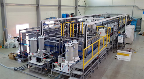
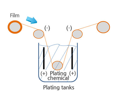
R to R Plating
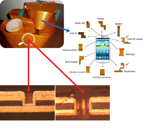
Other Services
-
EMI Shield Sputter
Basic Configuration of Sputter (1Chamber) — Sputtering Chamber + Carrier L/UL(Vacuum/Standby) + Baking Chamber + Cassette L/UL 01. Cassette L/UL02. Carrier L/UL
-
Wafer Plating
Application : Semiconductor Wafer Bumping RDL/UBM Process Cu Plating Process Cu Plating Equipment Composition Wafer Cu Plating Equipment 3D Design – Composition: