 We are Creating · Co-working · Contributing
We are Creating · Co-working · Contributing
We are Creating · Co-working · Contributing
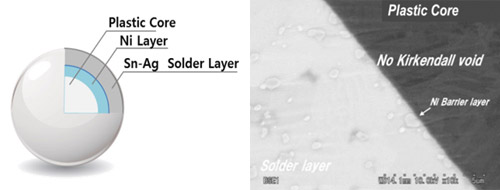
Plastic Cored Solder Ball

Other Services
-
Wafer Plating
Application : Semiconductor Wafer Bumping RDL/UBM Process Cu Plating Process Cu Plating Equipment Composition Wafer Cu Plating Equipment 3D Design – Composition:
-
R to R Sputter
R to R Sputter — Equipment to attract metallic/non metallic objects into film surfaces in vacuum chambers — Performance is given to