 We are Creating · Co-working · Contributing
We are Creating · Co-working · Contributing
We are Creating · Co-working · Contributing
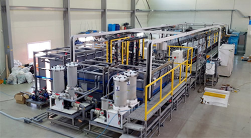
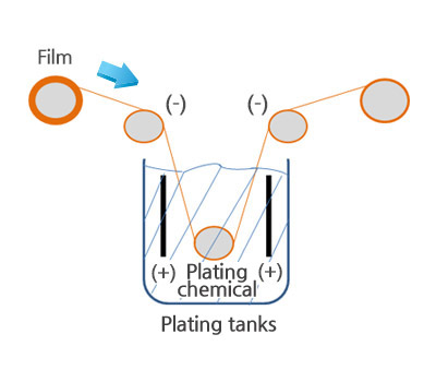
R to R Plating
Other Services
-
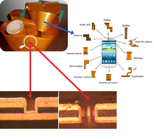
Screening/Radiator Film
Screening/Radiator Film — Shielding/heat radiation film deposition — Replace traditional plating with sputtering. Gain quality and price competitiveness by diversifying and simplifying
-
EMI Shield Sputter
Basic Configuration of Sputter (1Chamber) — Sputtering Chamber + Carrier L/UL(Vacuum/Standby) + Baking Chamber + Cassette L/UL 01. Cassette L/UL02. Carrier L/UL